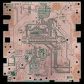
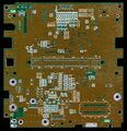
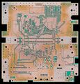
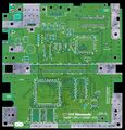
SNES Super Nintendo Entertainment System

From Repair Wiki

The second major console from Nintendo (Super Famicom in Japan, Super Nintendo in Europe and the USA), is the successor of the Famicom or Nintendo Entertainment System. It uses roughly the same hardware architecture as its predecessor, yet slightly improved.

SNES Super Nintendo Entertainment System
Manufacturer Nintendo
Code name SHVC
Release date 21. November 1990
Device type Game Console


Guides

Explanatory Guides

Repair Guides

Device pictures

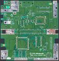
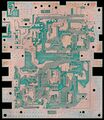
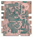
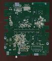
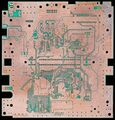
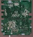
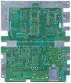
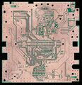
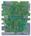
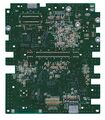
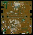
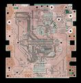
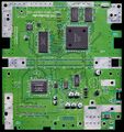
PCB pictures

HQ version

Reference measurements (also schematics if available)

More Information/External Sources

Schematics and Board-view

NTSC:

Schematic:

https://wiki.superfamicom.org/uploads/snes_schematic_color.pdf

PAL

Schematic:

https://wiki.console5.com/tw/images/f/fc/PAL-SNES_Schematic.pdf

Board-view:

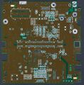
https://kicanvas.org/?github=https%3A%2F%2Fgithub.com%2FstonedDiscord%2FnonSNES

Points to note

  • Before you do anything on the device, it is wise to have a quick visual inspection around the board. Are there any signs of liquid damaged, corrosion, scratches, burn marks, or leaked capacitors? Also read the Visual Inspection page.
  • If this guide talks about replacing one of the bigger chips (PPU/CPU/WRAM), the chip can be replaced with any version of that chip. Multiple versions of the CPU, PPU1, PPU2, and WRAM chips have been made and these can be mixed and matched without issues. None of these chips are still in production so they will have to be salvaged from a donating device.
  • It helps tremendously if you can get your hands on a SNES Burn-In Test Cart. Unofficial ones can be bought through various channels like Amazon or AliExpress for cheap. They can test various hardware issues.
  • The power smoothing capacitor inside the device holds quite a charge after the device has been turned off (because the power switch is positioned between the rectifier and caps and the rest of the device). Make sure you discharge this capacitor before you work on the machine's insides, otherwise the power switch on wires can drop on the PCB and damage the chips. This can be done by turning on the device using the power switch while there is no power supply plugged in. The power LED will flash shortly if you do this.
  • There are basically two major architectures for the device. The multi-chip, and the single-chip (1CHIP) versions. The latter is the latest version and combines multiple chips (CPU and PPU) into one. The number printed on the PCB should clearly show if it's a 1CHIP version.

Metal inserts in case

At the bottom of the case, there are two metal inserts underneath the PCB. On the Super Famicom the front one is shaped slightly different because of the size of the board. These inserts have to be in the right orientation for external devices (like the SatellaView) to be screwed onto the console.

Screws

Five types of screws are used in the assembly. All but one are Phillips Head screws. The outer case screw has a security head and disassembly will require a special "Gamebit" screwdriver.

Guides
Problem Solution
No Power (LED off)
  • Make sure that none of the peripherals short the power rail. The power LED should light when you turn on the device even if there is no game cartridge, no AV cable, no RF cable, and no controller connected.
  • Check output voltage of the power adapter. This should be either 9V DC or AC.
  • If a DC power supply is used, check the correct polarization of the barrel jack of the Power Adapter. The (Japanese) Super Famicom uses a central Ground pin with a positive (9V) outer shell while the USA and European Super Nintendo uses a central positive (9V) pin and the barrel as ground. 9V AC should also work as the device rectifies the AC internally
  • Check continuity of the fuse (top left side of the board, near the power connector. The fuse is floating inside a cutout of the PCB.
  • Check output of the 7805 (located on the left side, attached to the heat sink)
  • Check that the input suppression choke (coil) has a low impedance.
No video signal at all
  • Check that the AV connector is clean
  • Check if the capacitors (you need to remove the heatsink) near the AV connector have not leaked
  • Check system clock on S-CLK (U18)
No video (signal, but black screen)
  • Make sure there is a working game cartridge that matches the region of the device is inserted properly (yes, sometimes problems are this simpel)
  • Make sure the cartridge slot is clean
  • Optically inspect the cartridge slot to make sure it has no bent pins. All pins should be identical.
  • Check that the /RESET line (pin 10 on the CIC chip (U8), 34 on PPU2 (U3)) is high after turning the device on (with a cartridge in). If it is not, the CIC chip may hold the RESET line low because it cannot communicate with the cartridge properly. Try cleaning the cartridge slot or try a different cartridge.
  • Check that the /RESOUT0 line (pin 33 on the PPU2 (U3)) and /RESOUT1 line (pin 28 on the PPU2 (U3)) are high after turning the device on (with a cartridge in). If they are low, while the /RESET line (see above) from the CIC chip (U8) is high), replace the PPU2 chip.
  • Check activity on the PPU2. Check if signals are output through the RGB and CSYNC output pins 95, 96, 97, and 100 of the PPU2 (U3). If there is no data, replace PPU2. If there is data, replace S-ENC (U7).
No audio
  • Check that the AV connector is clean
  • Check if the capacitors (you need to remove the heatsink) near the AV connector have not leaked
Garbled sprites
  • Replace PPU2.
Some sprites (like Mario in Super Mario World) don't show up while game plays perfectly.
  • This is an issue with the object overlay of the PPU1 chip. Replace the PPU1 chip. Using a burn-in test cartridge probably shows failures on OAM and/or OBJ L OVER. See table below.
A horizontal noise bar moves across the video output
  • Ground the shield of the RF output to a proper ground/earth and see if it disappears.
  • Place a 470uF cap across the G and O pins of the 7805 to filter out power supply noise.
  • If the device is powered using a non-original power supply, replace with a proper power supply
Left audio not working
  • Check if the trace (on the top side of the board) that runs underneath the C59 and C60 silk labels is corroded. Check its continuity between the vias. If it is not conducting, run a bodge wire on the bottom side of the board from R70 straight to a test point that is connected to C66 (see picture). Replace C59 with a 10uF/50V non-polarized electrolytic cap. The problem is caused by a leaking cap C59 that has eaten away the trace. On old boards, they designed in the wrong cap type. C59 and its neighbor C60 are used to provide +12V on the AV connector for peripherals that use power. Some AV-to-hdmi adapters use it. Leaving out C59 will only remove the 12V power from the AV connector and should not have side-effects.
RF output not working
  • RF output should be around 55.55MHz for PAL and 91.35MHz for NTSC-J.
  • Check with an oscilloscope if there is a signal on pin 7 of the S-ENC chip (U7).
  • If there is not a signal, check if U7 has 5V power on pin 5, and a clock signal on pin 14. If both signals are okay, U7 may be broken. replace U7 (S-ENC).
  • If U7 puts out a signal on its pin 7, check continuity between pin 7 of U7 and pin 2 of the RF module. The resistor R30 should also be connected to pin 7 on U7 and to pin 2 of the RF module. Check if C59 has leaked (see "Left audio not working" solution). Run a bodgewire from R30 to pin 2 of the RF module. R30 is at the bottom of the PCB. For the PAL version R30 is at the front side of the device, and you should use the side that is closest to the edge of the PCB. For the Japanese, R30 is at the back of the device, near the RF module's pins, and use the side that is farthest away from the edge of the PCB. It is best to check continuity to pin 7 of U7, just to be sure you have the correct side.
RESET button not working
  • Test if the reset switch properly bridges the front two pins when pushed. There are markings of 2 and 6 on top of the switch for above pins. Pushing the switch should lower the resistance to practically zero. If the contacts don't get bridged properly or if there is still resistance, spray some contact spray inside the switch from the top. If this does not help, replace the switch. Use a high powered soldering iron because the switch is connected to both the GND and the VCC plane which takes away a lot of the heat.
Incorrect colors - banding on the image
  • If incorrect colors are shown (a tinted image, not a grayscale image. A grayscale image is most likely a different issue), and there are horizontal lines across the overall image, the S-ENC (U7) chip needs replacing. There are two major types of S-ENC (U7) chips. They are identical in functionality but the supporting circuitry is different so they are not interchangeable without changing the circuitry around them too. There is a Nintendo branded S-ENC (9xxx) that is mostly used in PAL devices and some of the older NTSC devices, and the BA6592F chip that is used in most NTSC devices. The BA6592F doesn't bare the Nintendo logo, and you might be able to find those online, sometimes even new old stock.
SNES Burn-In Test Cart failures
Problem Solution
HV TIMER Replace CPU

Horizontal/Vertical sync timing used by some games and accessories (like the scope).

OAM Replace PPU1

Object Attribute Memory is part of PPU1.

OBJ L OVER Replace PPU1

Object overlay. /OVER signal is part of PPU1.

External links

https://wiki.console5.com/wiki/SNES

https://wiki.superfamicom.org/schematics-ports-and-pinouts

Some failure modes:

https://www.projectvb.com/nss/logs.htm