(One intermediate revision by the same user not shown)
Line 13:
Line 13:
* Blue screen of death
* Blue screen of death
* Usually frame will be bent
* Usually frame will be bent
[[File:Nintendo-Switch-Blue-Screen.jpg|alt=Nintendo Switch Blue Screen of Death|thumb|Blue screen of death on Nintendo Switch]]
[[File:Nintendo-Switch-Blue-Screen.jpg|alt=Nintendo Switch Blue Screen of Death|thumb|Figure 1: Blue screen of death on Nintendo Switch]]
=== Diagnostic Steps ===
=== Diagnostic Steps ===
BSOD on Nintendo switch is often due to the CPU or RAM not being able to properly communicate with the rest of the board because of cracked solder balls under the chip(s) or broken traces. The motherboard is very thin and a slight bend in the board will cause solder balls to get cracked or traces to become damaged. in the next steps we will try and determine which part of the board has these cracked solder balls or bad traces.
BSOD on Nintendo switch is often due to the CPU or RAM not being able to properly communicate with the rest of the board because of cracked solder balls under the chip(s) or broken traces. The motherboard is very thin and a slight bend in the board will cause solder balls to get cracked or traces to become damaged. in the next steps we will try and determine which part of the board has these cracked solder balls or bad traces.
[[File:3104-motherboard.jpg|thumb|502x502px|Figure 2: Nintendo Switch CPU (circled in blue) and RAM (Circled in red) locations.]]
* Observe if there is any bowing out of the board especially over the area around the CPU or RAM (See figure 1 for location of these chips)
* Observe if there is any bowing out of the board especially over the area around the CPU or RAM (See figure 2 for location of these chips)
* If there is bowing or bending over one of the chips then use your finger to put pressure over the IC in question and try to charge or turn on the console, if you get a Nintendo logo then we know that the issue is to due to the chip(s) we have just put pressure on. Keep in mind that sometimes you may have to put pressure on both RAM chips in order to get it to show Nintendo logo especially if the bent part of the board is over where the RAM chips are located.
* If there is bowing or bending over one of the chips then use your finger to put pressure over the IC in question and try to charge or turn on the console, if you get a Nintendo logo then we know that the issue is to due to the chip(s) we have just put pressure on. Keep in mind that sometimes you may have to put pressure on both RAM chips in order to get it to show Nintendo logo especially if the bent part of the board is over where the RAM chips are located.
* If you are still not getting it to show a Nintendo logo then you may want to try using your hot air station set to a low temp such as 150C-200C and heat up each IC for about 10-20 seconds and then try to turn the console on or plug it in to the charger in order to get a Nintendo Logo. Be careful not to damage the plastic frame or LCD doing this and only use low heat for a short amount of time if it's still in the frame
* If you are still not getting it to show a Nintendo logo then you may want to try using your hot air station set to a low temp such as 150C-200C and heat up each IC for about 10-20 seconds and then try to turn the console on or plug it in to the charger in order to get a Nintendo Logo. Be careful not to damage the plastic frame or LCD doing this and only use low heat for a short amount of time if it's still in the frame
Line 40:
Line 40:
Watch TheCod3r's video on solving this issue for a video breakdown on solving BSOD with a reflow here: https://www.youtube.com/watch?v=HdDvmxBl52I&t=660s
Watch TheCod3r's video on solving this issue for a video breakdown on solving BSOD with a reflow here: https://www.youtube.com/watch?v=HdDvmxBl52I&t=660s
==== Reball: ====
[[File:S9819c4021f5c49829def7223e2ab43f5S.webp|thumb|Figure 3: Amaoe magnetic base stencil]]
Reballing the CPU or RAM IC's will be a bit more difficult but if done correctly will make sure the problem never re-emerges unless too much stress is added to the board again. For doing this you will need a reballing stencil and for the CPU it's recommended that you get one that comes with a magnetic base to keep everything positioned correctly while applying solder paste and heating up the paste while in the stencil like the Amaoe one in figure 3. The RAM IC's are a bit easier to reball and can use a regular flat stencil without a magnetic base.
* If you haven't already from the reflow steps make sure to pull board out and remove the shield covering the CPU and RAM off and thoroughly clean the old thermal paste from the CPU.
* Take a picture or make sure to notate the orientation dot on the corner of the chip you're planning to remove so you know what orientation it needs to be in when installing it back on the board
* Same as reflow steps place a ring of flux around the CPU or RAM (again depending on which IC(s) were the problem
* Set your hot air to 375C-450C and medium airflow with the nozzle removed and start heating up the area around and on top of the chip you need to reball.
* Keep heating until you can bump the chip and it moves slightly before returning to the original position, this means the solder balls are melted and using a large pair of tweezers slowly lift the IC(s) off of the board
* Closely observe the board now that the IC has been removed to see if there are any ripped or loose pads. If there are you'll need to run a jumper to rebuild the pad that's missing
** Luckily most of the pads on the Switch board that seem to be prone to ripping have traces on the surface of the board that you can easily follow from where the pad was located
** Follow the trace up to a point where it's not loose and scrape away the coating covering it until you reach the copper trace.
** Solder a jumper wire or soldering lug to the exposed trace and run it to where the missing pad was located underneath the IC you just removed.
** Cover the exposed trace with UV conformal coating up to the rebuilt pad and harden it with a UV light
* To reball the IC first place some flux on the chip, then run your iron over the pads on the IC with low melt solder to try and get most of the pads to an equal smaller height.
** If the low melt solder is not enough to flatten out the solder on the chip then use soldering wick to completely flatten all of the pads after adding low melt.
** If using wick on the chip USE CAUTION with how much pressure you put into the wick with your iron as you can easily scrape and ruin the IC by wicking it. You'll want to barely touch the IC with your wick and have just enough pressure to remove the solder and flatten out the pads.
* Once the pads are flattened clean off the IC with iso and a cloth then place it into your stencil base (if using magnetic stencil from figure 2) or place the IC on a folded paper towel or rubber base, then position your stencil over the top of it making sure the holes in the stencil line up with the pads on the IC
* Evenly spread solder paste (Use a medium or low temp paste) in all of the holes of the stencil and then scrape the remaining paste off that's not in the holes of the stencil from the top of the stencil
* Using hot air on lower or medium airflow at 350-400C and a medium sized nozzle start heating the perimiter of the stencil in a circular motion and slowly start moving the hot air over the solder paste in the stencil until all of the paste turns into solder balls
** You may need to apply pressure to the top of the stencil in order the keep the stencil from warping
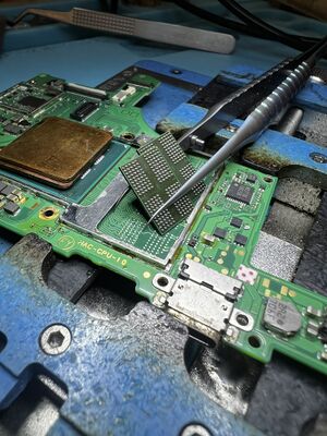
* [[File:08D2C23F-6BBF-46C6-A781-613F6FC0E2C1 1 102 o.jpeg|thumb|Figure 4: Both RAM ICs reballed in order to fix BSOD issue on Nintendo Switch]]Once you have reballed the IC(s) you'll need to prep the board to reinstall the freshly reballed IC(s)
** First add flux and with your iron and low melt solder start flattening out the pads on the board itself similar to what we did prepping the IC for reballing
** You will more than likely need to use a larger iron tip than what was used for the IC(s) as the motherboard itself is a large heatsink and a smaller iron tip won't have enough thermal mass to effectively melt the solder on the board especially on any ground pads.
** Once low melt solder has been added to all the pads on the board, use wick and your iron to completely flatten all the pads
** If you're not comfortable using your iron to wick the pads it may be a bit easier to use hot air to heat the wick and running the wick over the pads like a brush while heating it with hot air
** Clean the board of any remaining flux that is now stale due to the wicking process
** Add a very flattened out layer of flux to the pads (heating up the board prior to applying new flux helps spread the flux out a bit more evenly)
* Now that both our board is prepped and our IC(s) are reballed we can now position our freshly reballed chip on the board making sure to keep in mind where the orientation dot is located.
* Remove the nozzle again from your hot air and set it to a low to medium airflow with temperature at 375-425C and using a very slow circular motion start heating up the area around and on top of the IC until it can be lightly bumped with a tweezers and it moves back into its original spot. You can usually tell when the chip solder balls are melted and the chip is correctly in place when you can see the flux under the chip start "pulsing" on the perimeter. When the solder melts and attaches to the board, the chip will be pulled into the board a bit causing the flux to be pushed down and the heat from your hot air will cause the flux to make this "pulsing" motion on the bottom edge of the IC
* Wait for the board to cool down and clean all of the old flux off, then plug it in to make sure the problem is fixed and you no longer have a BSOD. Then add new thermal paste to the top of the CPU, place the shield back over the CPU and RAM, and then make sure to place new thermal paste again between the CPU shield and the heat sink.
* If you still have BSOD then you either have not done the reball correctly or you have additional problems with the other IC(s) that you didn't reball, or even a ripped or loose pad that was missed. In somewhat rare cases a faulty EMMC can also cause BSOD but it's usually going to be CPU or RAM
multimeter, soldering iron, soldering station, BGA rework station
Difficulty
◉◉◉◉ Specialist
Type
BGA, Soldering
Problem Description
Nintendo switch will only show a blue screen when charging, turning on etc. Usually will happen when the device is bent or bowed out in the middle
Symptoms
Blue screen of death
Usually frame will be bent
Figure 1: Blue screen of death on Nintendo Switch
Diagnostic Steps
BSOD on Nintendo switch is often due to the CPU or RAM not being able to properly communicate with the rest of the board because of cracked solder balls under the chip(s) or broken traces. The motherboard is very thin and a slight bend in the board will cause solder balls to get cracked or traces to become damaged. in the next steps we will try and determine which part of the board has these cracked solder balls or bad traces.
Figure 2: Nintendo Switch CPU (circled in blue) and RAM (Circled in red) locations.
Observe if there is any bowing out of the board especially over the area around the CPU or RAM (See figure 2 for location of these chips)
If there is bowing or bending over one of the chips then use your finger to put pressure over the IC in question and try to charge or turn on the console, if you get a Nintendo logo then we know that the issue is to due to the chip(s) we have just put pressure on. Keep in mind that sometimes you may have to put pressure on both RAM chips in order to get it to show Nintendo logo especially if the bent part of the board is over where the RAM chips are located.
If you are still not getting it to show a Nintendo logo then you may want to try using your hot air station set to a low temp such as 150C-200C and heat up each IC for about 10-20 seconds and then try to turn the console on or plug it in to the charger in order to get a Nintendo Logo. Be careful not to damage the plastic frame or LCD doing this and only use low heat for a short amount of time if it's still in the frame
Solution
Now that we have determined which chip(s) are causing the BSOD we can move on to determining the best method of repair for your individual circumstances.
Reflow:
Reflowing the solder under the IC in question will by far be the easiest method of fixing the problem albeit this will usually be a temporary fix. However if you dont have the appropriate knowledge, tools, or experience doing a reball then a reflow will be a good option. Keep in mind a reflow will also not always fix the issue especially if there are damaged traces.
First remove the board from the housing and then remove the shield covering CPU and RAM if you haven't already by pulling the clips off from around the shield
Next clean off the old thermal paste covering the CPU with isopropyl. If the thermal paste is left it will make the reflow uneven especially if you are reflowing the CPU and not the RAM
Place a ring of flux paste around the CPU or RAM
Set your hot air to a temp around 375-450C and medium airflow with the nozzle off and with a circular motion start heating up the area of the CPU or RAM
Keep applying heat until you can slightly nudge the IC with a tweezers and have it move a tiny bit but then move back to the original position, this means the Solder balls underneath are fully melted and have been reflowed.
Remove heat and clean up the remaining flux with iso while waiting for the board to cool down
Once board has cooled down, put it back into the housing and test to see if it turns back on again without a blue screen of death. If it still has a blue screen then you have not solved the issue and you should move on to the reball steps below or try reflowing the opposite chip(s) to what you just reflowed.
if it turns on fine without BSOD then fully reassemble making sure to add new thermal paste between the shield and CPU as well as between the heat sink and CPU shield
Reballing the CPU or RAM IC's will be a bit more difficult but if done correctly will make sure the problem never re-emerges unless too much stress is added to the board again. For doing this you will need a reballing stencil and for the CPU it's recommended that you get one that comes with a magnetic base to keep everything positioned correctly while applying solder paste and heating up the paste while in the stencil like the Amaoe one in figure 3. The RAM IC's are a bit easier to reball and can use a regular flat stencil without a magnetic base.
If you haven't already from the reflow steps make sure to pull board out and remove the shield covering the CPU and RAM off and thoroughly clean the old thermal paste from the CPU.
Take a picture or make sure to notate the orientation dot on the corner of the chip you're planning to remove so you know what orientation it needs to be in when installing it back on the board
Same as reflow steps place a ring of flux around the CPU or RAM (again depending on which IC(s) were the problem
Set your hot air to 375C-450C and medium airflow with the nozzle removed and start heating up the area around and on top of the chip you need to reball.
Keep heating until you can bump the chip and it moves slightly before returning to the original position, this means the solder balls are melted and using a large pair of tweezers slowly lift the IC(s) off of the board
Closely observe the board now that the IC has been removed to see if there are any ripped or loose pads. If there are you'll need to run a jumper to rebuild the pad that's missing
Luckily most of the pads on the Switch board that seem to be prone to ripping have traces on the surface of the board that you can easily follow from where the pad was located
Follow the trace up to a point where it's not loose and scrape away the coating covering it until you reach the copper trace.
Solder a jumper wire or soldering lug to the exposed trace and run it to where the missing pad was located underneath the IC you just removed.
Cover the exposed trace with UV conformal coating up to the rebuilt pad and harden it with a UV light
To reball the IC first place some flux on the chip, then run your iron over the pads on the IC with low melt solder to try and get most of the pads to an equal smaller height.
If the low melt solder is not enough to flatten out the solder on the chip then use soldering wick to completely flatten all of the pads after adding low melt.
If using wick on the chip USE CAUTION with how much pressure you put into the wick with your iron as you can easily scrape and ruin the IC by wicking it. You'll want to barely touch the IC with your wick and have just enough pressure to remove the solder and flatten out the pads.
Once the pads are flattened clean off the IC with iso and a cloth then place it into your stencil base (if using magnetic stencil from figure 2) or place the IC on a folded paper towel or rubber base, then position your stencil over the top of it making sure the holes in the stencil line up with the pads on the IC
Evenly spread solder paste (Use a medium or low temp paste) in all of the holes of the stencil and then scrape the remaining paste off that's not in the holes of the stencil from the top of the stencil
Using hot air on lower or medium airflow at 350-400C and a medium sized nozzle start heating the perimiter of the stencil in a circular motion and slowly start moving the hot air over the solder paste in the stencil until all of the paste turns into solder balls
You may need to apply pressure to the top of the stencil in order the keep the stencil from warping
Figure 4: Both RAM ICs reballed in order to fix BSOD issue on Nintendo SwitchOnce you have reballed the IC(s) you'll need to prep the board to reinstall the freshly reballed IC(s)
First add flux and with your iron and low melt solder start flattening out the pads on the board itself similar to what we did prepping the IC for reballing
You will more than likely need to use a larger iron tip than what was used for the IC(s) as the motherboard itself is a large heatsink and a smaller iron tip won't have enough thermal mass to effectively melt the solder on the board especially on any ground pads.
Once low melt solder has been added to all the pads on the board, use wick and your iron to completely flatten all the pads
If you're not comfortable using your iron to wick the pads it may be a bit easier to use hot air to heat the wick and running the wick over the pads like a brush while heating it with hot air
Clean the board of any remaining flux that is now stale due to the wicking process
Add a very flattened out layer of flux to the pads (heating up the board prior to applying new flux helps spread the flux out a bit more evenly)
Now that both our board is prepped and our IC(s) are reballed we can now position our freshly reballed chip on the board making sure to keep in mind where the orientation dot is located.
Remove the nozzle again from your hot air and set it to a low to medium airflow with temperature at 375-425C and using a very slow circular motion start heating up the area around and on top of the IC until it can be lightly bumped with a tweezers and it moves back into its original spot. You can usually tell when the chip solder balls are melted and the chip is correctly in place when you can see the flux under the chip start "pulsing" on the perimeter. When the solder melts and attaches to the board, the chip will be pulled into the board a bit causing the flux to be pushed down and the heat from your hot air will cause the flux to make this "pulsing" motion on the bottom edge of the IC
Wait for the board to cool down and clean all of the old flux off, then plug it in to make sure the problem is fixed and you no longer have a BSOD. Then add new thermal paste to the top of the CPU, place the shield back over the CPU and RAM, and then make sure to place new thermal paste again between the CPU shield and the heat sink.
If you still have BSOD then you either have not done the reball correctly or you have additional problems with the other IC(s) that you didn't reball, or even a ripped or loose pad that was missed. In somewhat rare cases a faulty EMMC can also cause BSOD but it's usually going to be CPU or RAM