More actions
(Repair Guide For no charging) |
Hlyan Htet (talk | contribs) (no power) |
||
| (One intermediate revision by one other user not shown) | |||
| Line 1: | Line 1: | ||
{{Repair Guide | {{Repair Guide | ||
|Device= | |Device=Redmi Note 13 4G | ||
|Affects parts= | |Affects parts=Logic Board | ||
|Needs equipment= | |Needs equipment=Soldering Iron, Hot Air Station, Microscope | ||
|Type= | |Type=Soldering, BGA | ||
|Difficulty= | |Difficulty=3. Hard | ||
}} | }} | ||
{{stub}} | |||
== Problem description == | == Problem description == | ||
<!-- | <!-- | ||
| Line 49: | Line 50: | ||
* Remove the OVP IC | * Remove the OVP IC | ||
* Probe the pads to see there is no short to ground | * Probe the pads to see there is no short to ground | ||
* if everything is ok then proceed to make a jumper bypass the OVP IC from VBUS _ OVP _ INPUT to VBUS _ OVP _ OUTPUT (shown in the picture below) | * if everything is ok then proceed to make a jumper bypass the OVP IC from VBUS _ OVP _ INPUT to VBUS _ OVP _ OUTPUT | ||
* (shown in the picture below) | |||
[[File:BYPASS OVP.png|center|thumb|BYPASS OVP IC]] | [[File:BYPASS OVP.png|center|thumb|BYPASS OVP IC]] | ||
* Test if everything is working | * Test if everything is working | ||
Latest revision as of 20:20, 21 March 2026
| Redmi Note 13 4G Not Charging | |
|---|---|
| Device | Redmi Note 13 4G |
| Affects part(s) | Logic Board |
| Needs equipment | Soldering Iron, Hot Air Station, Microscope |
| Difficulty | ◉◉◉◌ Hard |
| Type | Soldering, BGA |
This article is a stub. You can help Repair Wiki grow by expanding it
Problem description
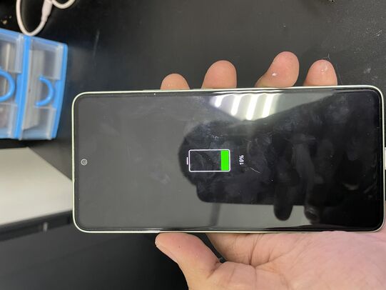
The device works fine, turn on and its fully functional but does not achrge at all and the charging is not even detected.
Symptoms
- Phone works but does not charge.
- Turns on with new battery
- Diode value on main connector is ok
- Charging is not detected in on state or off state
- Draw on AMP meter is 0.000V
Solution
Mainly this issue occurs with a faulty charger aur cable, in the result of this the device blows its OVP(Over Voltage Protection) ic to keep the device safe.
Note: Replacement of charger and charging cable is recommended after the repair.
Diagnostic Steps
To check all the voltages you have to plugin only the charger, battery is not required to check the following voltages.
- Measure diode value on the charging FPC connector
- Check voltage on VBUS 5.0 volt
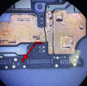
- If 5.0 volt is present on the VBUS line then proceed to check the following components
- Check if ovp ic is working:
- Check the VBUS IN if is providing 5.0v
- Check the VBUS OUT if its porviding the 5.0v output
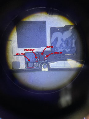
- If the VBUS OUT 5.0v is missing then proceed to the repair steps below.
Repair Steps
- Remove the OVP IC
- Probe the pads to see there is no short to ground
- if everything is ok then proceed to make a jumper bypass the OVP IC from VBUS _ OVP _ INPUT to VBUS _ OVP _ OUTPUT
- (shown in the picture below)
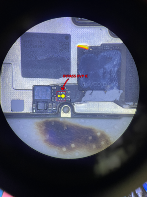
- Test if everything is working
- Apply solder mask and your device should be ready
