
More actions
Size of this preview: 800 × 600 pixels. Other resolutions: 2,560 × 1,920 pixels | 8,000 × 6,000 pixels.
Original file (8,000 × 6,000 pixels, file size: 5.32 MB, MIME type: image/jpeg)
Summary
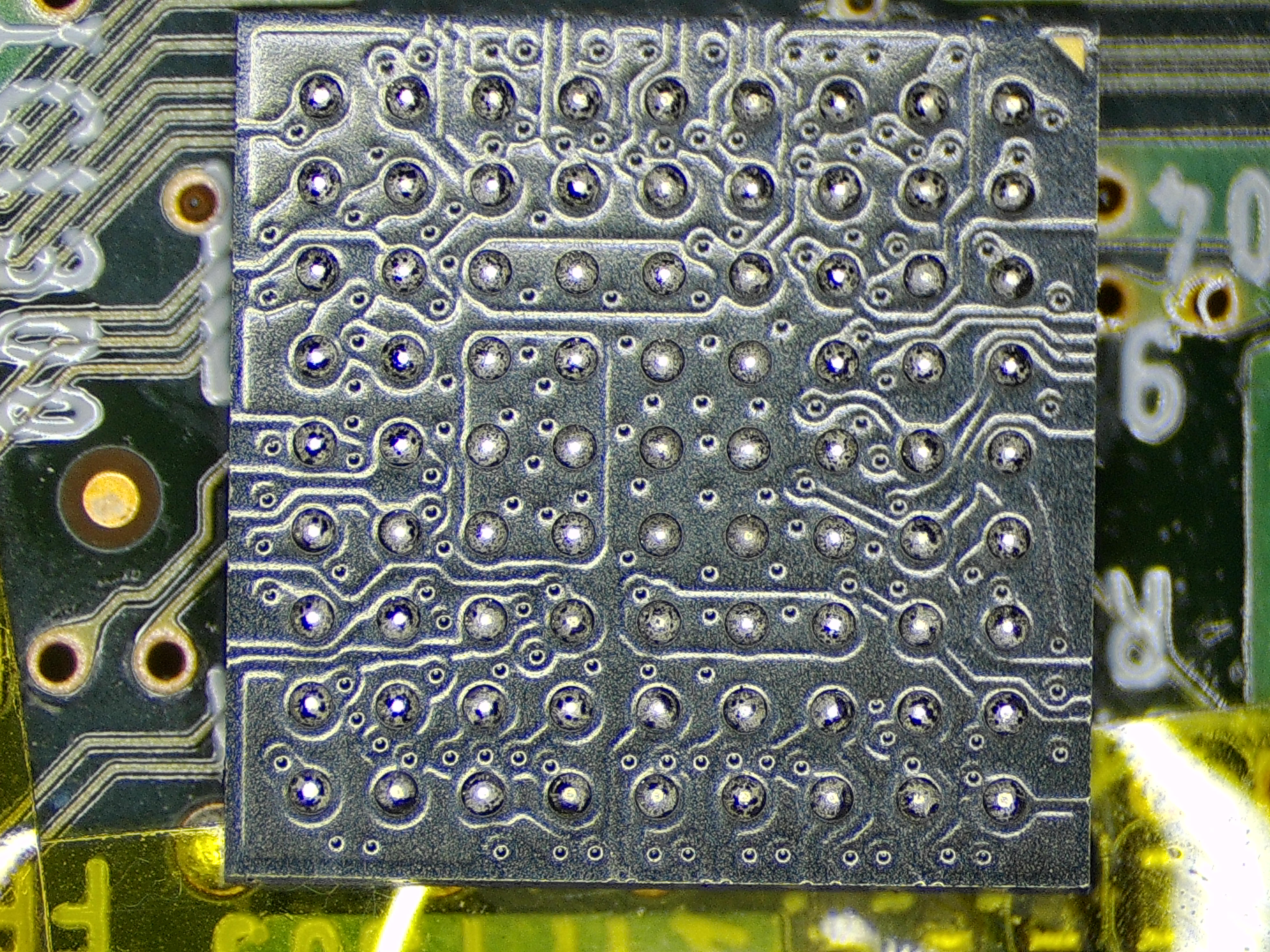
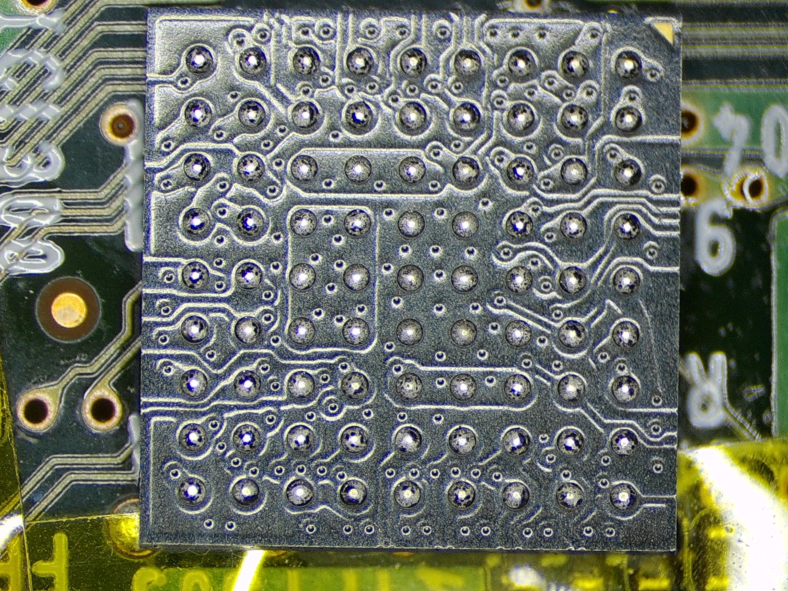
This is a high resolution image of what the THP7312 chip's bottom layer substrate looks like. May be useful for future reverse engineering.
File history
Click on a date/time to view the file as it appeared at that time.
| Date/Time | Thumbnail | Dimensions | User | Comment | |
|---|---|---|---|---|---|
| current | 13:53, 14 January 2024 | | 8,000 × 6,000 (5.32 MB) | Pandrew (talk | contribs) | This is a high resolution image of what the THP7312 chip's bottom layer substrate looks like. May be useful for future reverse engineering. |
You cannot overwrite this file.
File usage
The following page uses this file: