More actions
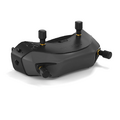
| Avatar HD Goggles | |
|---|---|
| Manufacturer | Walksnail |
| Code name | |
| Release date | |
| Device type | Drone |
This article is a stub. You can help Repair Wiki grow by expanding it
Guides
Explanatory Guides
Repair Guides
Create a Guide
Device pictures
PCB pictures
-
Avatar FPV Goggles PCB
-
-
-
-
-
-
-
-
-
-
-
Reference measurements (also schematics if available)
Please consider contributing pictures to this section!
More Information/External Sources
Walksnail Avatar HD fpv goggles are also sold as Fat Shark Dominator HD FSV1125
https://walksnail.com/
https://www.fatshark.com/
About The System
The Avatar HD Goggles are a new digital FPV goggle made by Walksnail part of CaddX FPV.
These Goggles have been made in partnership with Fat Shark and are sold under both the Fat Shark and Walksnail brand.
They are both compatible with the Walksnail Avatar HD VTX and offer same/similar functionally.
Walksnail Avatar HD fpv goggles are also sold as Fat Shark Dominator HD FSV1125
https://walksnail.com/ - https://www.fatshark.com/
About The System:
The Avatar HD Goggles are a new digital FPV goggle made by Walksnail part of CaddX FPV.
These Goggles have been made in partnership with Fat Shark and are sold under both the Fat Shark and Walksnail brand.
They are both compatible with the Walksnail Avatar HD VTX and offer same/similar functionally.
Important SOC Images Notes:
The main SOC is labelled as a Xilinx Virtex 5 XC5VLX50T - FFG1136FGU2033 - AC4284883A1 2C.
Based on code samples and SOC package it is strongly believed this is not this FPGA. Its believed to be a Artosyn RF Chipset such as the AR9201/AR8211.
Specification
AR9201
Application Processor Core
1.5GHz ARM Cortex-A7 quad-core, each core with 32KB I-cache, 32KB D-cache
512KB L2 cache
Neon acceleration and double precision FPU
Embedded Trace data interface (16KB ETB) for ARM-DS5 debugger
DVFS control: Dynamic voltage and frequency scaling to reduce power consumption
MCU core
500MHz CPU, 16Kbyte I-cache, 16KB D-cache
128KB ITCM and 64KB DTCM
Double precision FPU
CEVA DSP core
4 x high performance CEVA XM4 Cores at 1000MHz
2M-Byte shared on-chip SRAM
Video Codec Format
H.264 BP/MP/HP encoding and decoding
H.265 MAIN/MAIN10 @L5.0 High-tier encoding and decoding
MJPEG/JPEG Extended Sequential encoding and decoding
Video Codec Performance
Software configurable video codec, either as encoder or as decoder
Real-time multi-stream H.264/H.265 encoding or decoding:
H.264: [/cdn-cgi/l/email-protection [email protected]]
[/cdn-cgi/l/email-protection [email protected]][/cdn-cgi/l/email-protection [email protected]]
MJPEG/JPEG encoding/decoding at [/cdn-cgi/l/email-protection [email protected]]
MJPEG/JPEG encoding and decoding
Baseband
2T4R with 2.5MHz/5MHz/10MHz/20MHz/40MHz bandwidth
BPSK/QPSK/16QAM/64QAM/256QAM modulation
LDPC encoder with 1/2, 2/3, 3/4 code rate
Max down link rate at 100Mbps
2.4G/5.8G uplink/downlink communication
One AP support max to four nodes
Analog
One 8-1 10bit SAR ADC
Two 10bit SAR ADCs
Four 12bit DACs
Eight 12bit ADCs
Peripherals
9 UARTs
2 Watch dog timers
20 timers,10 of which have PWM output
4 CAN bus interface
5 I2C interfaces, can be configured as either master or slave by software
4 SPI masters(2x1-1, 2x1-5 ), 2 SPI slave
4 I2S 4bit interfaces
147 GPIO, shared with other functions.
2 AXI DMA controller
One AHB DMA controller
USB 3.0 DRD controller and PHY.
USB 3.0 /Type-C / DisplayPort combo interface
10 /100/1000M Ethernet RGMII interface
2-lane PCIe 2.0, can be configured as EP or RC mode
External Memory Interfaces
DDR4/DDR3/LPDDR3 interface
16/32/64-bit DDR4 interface up to DDR4 2400
16/32/64-bit DDR3L interface up to DDR3L 2133
32/64-bit LPDDR3 interface up to LPDDR3 2133
SPI NOR flash interface
1-/2-/4-wire mode
3-byte or 4-byte address mode
Maximum capacity of 256 MB NOR flash or MCP SPI NOR+NAND flash
eMMC 5.1 interface with 64GB max capacity
Secure Boot from internal ROM with eMMC flash or SPI NOR flash.
Physical Specification
Power consumption
3W typical power consumption in the 4Kx2K scenario
Multiple power domains for power saving
[11:19]
Operating voltages
0.9V core voltage
1.8VI/O voltage
1.2V/1.2V/1.5V for DDR4/LPDDR3/DDR3(L)
3.3VI/O voltage
Package
FCBGA
Body size of 19mm x19mm
Ball pitch of 0.65mm


