
More actions
Showing below up to 50 results in range #1,151 to #1,200.
-
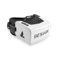 Fat shark scout hd goggles.jpg 1,000 × 1,000; 60 KB
-
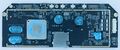 Fatshark Avatar Goggles PCB Front Main.jpg 4,747 × 1,993; 1.57 MB
-
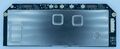 Fatshark Avatar Goggles PCB Front Shield.jpg 5,184 × 2,134; 1.58 MB
-
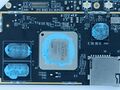 Fatshark Avatar Goggles PCB SOC.jpg 5,184 × 3,888; 1.58 MB
-
 Fatshark Avatar Goggles RAM.jpg 3,024 × 4,032; 1.64 MB
-
 Faulty heatsink.png 575 × 681; 535 KB
-
 Fcam.png 1,813 × 2,127; 5.31 MB
-
 Fig. 1.jpg 436 × 509; 250 KB
-
 Fig. 2 Notepad ++ Wrong SREC Checksum.jpg 537 × 579; 272 KB
-
 Fig. 3.jpg 1,011 × 537; 322 KB
-
 Fig. 4.jpg 968 × 526; 310 KB
-
 Fig. 5.jpg 305 × 533; 194 KB
-
 Fig. 6.jpg 679 × 709; 470 KB
-
 Files save 1.png 883 × 156; 23 KB
-
 Files save 2.png 705 × 500; 22 KB
-
 Finally. Xbox one headset adaptor.jpg 1,024 × 1,024; 82 KB
-
 FindFlashMediaAndKeepout.jpg 1,280 × 1,498; 128 KB
-
 Finger.png 934 × 1,331; 1.75 MB
-
 Finger Print Option.png 347 × 766; 42 KB
-
 Fingerprint tool.png 942 × 424; 413 KB
-
 Fixed.png 3,024 × 4,032; 12.52 MB
-
 Flash Renesas MCU.webp 765 × 160; 4 KB
-
 Flash capacitor.jpg 662 × 496; 49 KB
-
 Flex Adapter.png 203 × 207; 48 KB
-
 Flex Connected.png 243 × 485; 44 KB
-
 Flex dualsense.png 712 × 710; 273 KB
-
 Flex iPad.png 203 × 207; 48 KB
-
 Fold 4 USB Reading.jpg 1,536 × 2,048; 335 KB
-
 Fpc 1 and 2 S21 FE.jpg 4,032 × 3,024; 3.54 MB
-
 Front-cam-only.png 2,000 × 2,000; 881 KB
-
 Front-camera.png 2,000 × 2,000; 4.84 MB
-
 Front 3.3 short pascal.jpg 2,560 × 1,047; 644 KB
-
 Front 5V shorts on pascal GPUs.jpg 2,560 × 1,047; 657 KB
-
 Front USB FPC.png 1,372 × 1,830; 1.62 MB
-
-
 Front coils diode value a326.png 2,850 × 2,091; 8.62 MB
-
 Full light.png 2,112 × 3,684; 4.84 MB
-
 Fuse.png 132 × 70; 19 KB
-
 FviEqetk.jpg 1,768 × 2,040; 465 KB
-
 G27C4X how to remove flex cable.png 687 × 675; 645 KB
-
 GOggles-X-VRX-Module-Bottom-scaled.jpg 2,560 × 1,437; 395 KB
-
 GP102 1.8V Short.jpg 1,280 × 960; 541 KB
-
 GP104 1.8V Short.jpg 450 × 338; 22 KB
-
 GSM ANTENNA.jpg 4,032 × 3,024; 3.28 MB
-
 GTX 1080.jpg 2,560 × 1,047; 655 KB
-
 GX650PY PCB front.jpg 3,872 × 2,592; 4.17 MB
-
 Galaxy-A12-SM-A125F.png 344 × 515; 243 KB
-
 Galaxy-A32.png 700 × 700; 441 KB
-
 GalaxyA71.webp 450 × 568; 35 KB
-
 Galaxy A03s A037F PCB Back.jpg 595 × 417; 95 KB


.jpg)