More actions
(repair guide for no touch and display) |
(added 1 last photo) |
||
| Line 26: | Line 26: | ||
[[File:2025 05 13 15 19 IMG 77781-Recovered.png|thumb| | [[File:2025 05 13 15 19 IMG 77781-Recovered.png|thumb|175x175px|check diode values on these pads]] | ||
=== Diagnostic Steps === | === Diagnostic Steps === | ||
| Line 37: | Line 37: | ||
'''Start Removing the shield and trace the damage''' | '''Start Removing the shield and trace the damage''' | ||
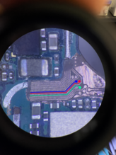
[[File:2025 05 13 11 44 IMG 7766.png|thumb| | [[File:2025 05 13 11 44 IMG 7766.png|thumb|149x149px|find the problem]] | ||
# Start by removing or grinding the front baseband section and CPU shields. | # Start by removing or grinding the front baseband section and CPU shields. | ||
| Line 43: | Line 43: | ||
'''Start the repair process''' | '''Start the repair process''' | ||
[[File:2025 05 13 12 27 IMG 7768.png|thumb| | [[File:2025 05 13 12 27 IMG 7768.png|thumb|163x163px|prep the damaged area]] | ||
# Start by removing the first layer of the motherboard(that is ground) on the area where your issue is located, it would be near the marked area. (to remove the 1st layer you can use a surgical blade #11 and be patient) | # Start by removing the first layer of the motherboard(that is ground) on the area where your issue is located, it would be near the marked area. (to remove the 1st layer you can use a surgical blade #11 and be patient) | ||
| Line 50: | Line 50: | ||
'''Soldering process''' | '''Soldering process''' | ||
[[File:2025 05 13 14 14 IMG 7769.png|thumb| | [[File:2025 05 13 14 14 IMG 7769.png|thumb|165x165px|fixed damaged area]] | ||
* I personally use a little bit of no halogen flux for this repair and use 183 C paste | * I personally use a little bit of no halogen flux for this repair and use 183 C paste | ||
| Line 59: | Line 59: | ||
'''More details about the pads''' | '''More details about the pads''' | ||
[[File:Touch and display pads.png|thumb|219x219px|pads info on the back]] | |||
* here is some more information about these pads from where the actually go and where the lead. | * here is some more information about these pads from where the actually go and where the lead. | ||
* | * | ||
[[File:2025 05 13 15 19 IMG 7778.png|thumb| | [[File:2025 05 13 15 19 IMG 7778.png|thumb|212x212px|pads info on the fpc]] | ||
enjoy, your repair has been successful.is completed. | enjoy, your repair has been successful.is completed. | ||
Revision as of 21:57, 4 June 2025
This article is a stub. You can help Repair Wiki grow by expanding it
Problem description
You have tried to replace the main FPC connector and display and the problem persists then this would be your issue.
The device has no touch after a little time of use OR no Touch at all.
The Device turns on normally but doesn't display anything.
Mainly this issue occurs after a heavy drop or if a customer drops his phone a lot.
Symptoms
- This issue happened after a drop
- You will experience no touch or no display or both at the same time but the phone is working and charging fine.
Solution

Diagnostic Steps
- Mainly this issue occures after a heavy drop
- Check diode readings on the following lines, if you have OL or high diode values at these pins then you should follow this guide.
Repair Steps
Warning: Attempting this repair without enough experience with microsoldering, may lead to a dead/ no dispay issue. Proceed with caution.
Start Removing the shield and trace the damage

- Start by removing or grinding the front baseband section and CPU shields.
- After you have carefully removed the shields try to trace the area where the problem has occured. (as shown in the picture)
Start the repair process

- Start by removing the first layer of the motherboard(that is ground) on the area where your issue is located, it would be near the marked area. (to remove the 1st layer you can use a surgical blade #11 and be patient)
- After you have successfully removed the 1st layer you can try to find the second layer and in that layer you will find the problem that is caused by a hard drop. (you will finds something like this picture)
Soldering process

- I personally use a little bit of no halogen flux for this repair and use 183 C paste
- prep the pads that are broken white tin and start jumpering the broken traces, I preffer to use 0.007mm silver jumper wire for these kind of works.
- After you have made the traces with jumper wire try to turn on the device and see if touch works properly and you have a display.
- If everything seems fine then now you are ready to apply a UV Solder Mask to finish the repair. (the end result should look like the picture.)
More details about the pads

- here is some more information about these pads from where the actually go and where the lead.

enjoy, your repair has been successful.is completed.
