
More actions
(S20 Diode Mode Readings) |
Tiago199988 (talk | contribs) |
||
| (2 intermediate revisions by 2 users not shown) | |||
| Line 11: | Line 11: | ||
== Device pictures == | == Device pictures == | ||
<gallery showthumbnails="1"> | <gallery showthumbnails="1"> | ||
File: | File:S20-768x768.webp|alt= | ||
</gallery> | </gallery> | ||
== PCB pictures == | == PCB pictures == | ||
<gallery showthumbnails="1"> | <gallery showthumbnails="1"> | ||
File: | File:S20 Front Board.png|Samsung S20 - Front of the Motherboard | ||
File:S20 Back Board.png|Samsung S20 - Back of the Motherboard | |||
</gallery> | </gallery> | ||
| Line 33: | Line 34: | ||
== More Information/External Sources == | == More Information/External Sources == | ||
<!-- | Galaxy S20 Schematics: https://www.sendspace.com/file/n9na4k<!-- | ||
You can manually link to external sources for additional information that might not fit here but are useful such as BIOS image dumps, firmware, etc! | You can manually link to external sources for additional information that might not fit here but are useful such as BIOS image dumps, firmware, etc! | ||
--> | --> | ||
Latest revision as of 20:16, 7 September 2025
| Galaxy S20 | |
|---|---|
| Manufacturer | Samsung |
| Code name | |
| Release date | |
| Device type | Phone |
This article is a stub. You can help Repair Wiki grow by expanding it
Guides
Explanatory Guides
| Type | Difficulty | |
|---|---|---|
| How to use ODIN to flash firmware on Samsung devices | Troubleshooting/Diagnostics |
Repair Guides
Create a Guide
Device pictures

PCB pictures
-
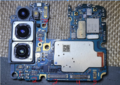
Samsung S20 - Front of the Motherboard
-
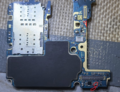
Samsung S20 - Back of the Motherboard


Reference measurements (also schematics if available)
-
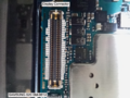
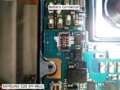
S20 Display FPC
-
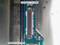
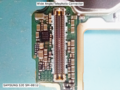
S20 Charging Flex FPC
-
S20 Battery FPC
-
S20 Wide Telephoto Cam FPC
-
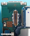
S20 UWCam FPC
-
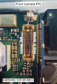
S20 Front Cam FPC
-
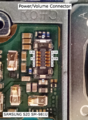
S20 Power Volume Button FPC
-
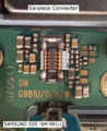
S20 Ear Speaker FPC
-
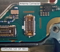
S20 Antenna FPC


More Information/External Sources
Galaxy S20 Schematics: https://www.sendspace.com/file/n9na4k